Technology Preview – SPIE Advanced Lithography Symposium 2025
Angie Kellen, Director, Client Services, Open Sky Communications
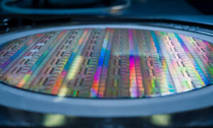
Semiconductor wafer Source: Coherent
With the semiconductor industry’s persistent push for smaller, more powerful, and energy-efficient chips, how can we meet this demand? Lithography and wafer patterning are pivotal processes of semiconductor manufacturing, enabling the fabrication of complex integrated circuits (ICs) with nanometer-scale precision. If you are not familiar with lithography and wafer patterning, these processes define the size, shape, and placement of transistors, interconnects, and other critical components, directly impacting chip performance, power consumption, and cost efficiency. Without continuous advancements in lithography, the industry would struggle to meet the growing demand for more powerful computing, efficient AI processors, next-generation mobile devices and so much more.
Actually, the demand for innovative lithography and patterning solutions has never been greater. As the relentless pursuit of Moore’s Law challenges traditional scaling methods, advanced lithography techniques, such as Extreme Ultraviolet (EUV) lithography, have become critical to achieving next-generation device architectures. With the rise of AI, 5G, and high-performance computing, chip manufacturers require precise, high-resolution patterning solutions to maintain performance improvements all while reducing costs. In addition, the shift to the 2nm node and beyond demands breakthroughs in photoresists, materials, and etching techniques, making innovation in lithography an essential enabler of future technology.

San Jose, California Source: SPIE Advanced Lithography + Patterning Symposium
It is this scenario that makes the SPIE Advanced Lithography + Patterning Symposium (SPIE-AL) so very important to the semiconductor industry, and in turn, every device manufacturer that uses a chip. This year it’s being held next week from February 23rd to the 27th at the San Jose McEnery Convention Center in San Jose, California. It is the key event for semiconductor professionals involved in the ecosystem around lithography and wafer patterning. This symposium brings together experts from around the globe to discuss challenges and share breakthroughs in lithography, patterning technologies, metrology, and process integration. In this blog, I will provide a high-level glimpse into the technologies that will be featured at SPIE-AL.
SPIE-AL is made up of six specialized conferences, each focusing on a critical aspect of lithography and patterning. Optical and EUV Nanolithography delves into the latest developments in optical and extreme ultraviolet (EUV) lithography techniques. DTCO and Computational Patterning explores design-technology co-optimization and computational methods to enhance patterning processes. The Metrology, Inspection, and Process Control segment focuses on advanced techniques for measuring and controlling processes to ensure precision in semiconductor manufacturing. Novel Patterning Technologies investigates emerging patterning methods that push the boundaries of current technology. The Advances in Patterning Materials and Processes segment examines new materials and processes that contribute to improved patterning performance. And Advanced Etch Technology and Process Integration for Nanopatterning discusses cutting-edge etching technologies and their integration into nanopatterning workflows.
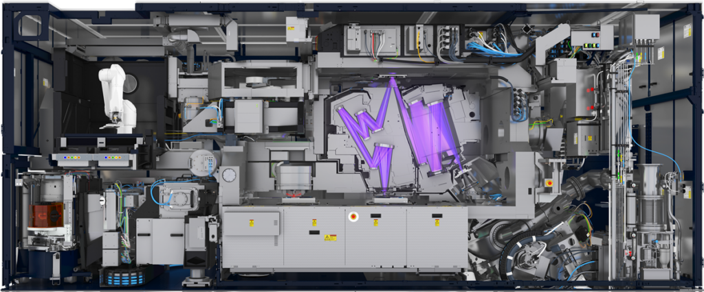
EUV Lithography system (ASML) Source: APP Economy Insights
In addition, the SPIE-AL symposium includes five topical tracks that offer attendees the opportunity to dive further into specific areas of interest. The Artificial Intelligence and Machine Learning (AI/ML) track explores the integration of AI and ML in enhancing lithography processes and outcomes. A somewhat new focus is Stochastics. This track examines the role of randomness in patterning and strategies to manage its effects. The Edge Placement Error (EPE) / Overlay track will discuss methods to minimize discrepancies in pattern alignment and placement. There is also the Advanced Packaging track, which will explore the intersection of lithography and heterogeneous integration, including novel patterning approaches for wafer-level packaging and 3D stacking. And a topic of increasing importance, Sustainability. This track addresses environmental considerations and sustainable practices in lithography and wafer patterning.
So much technology, so little time! EUV lithography is THE hot topic. And it is also the catalyst for new innovations around the ecosystem of technologies needed to support and propel EUV lithography to the next level. You can go to the full program to map out your schedule at the symposium. If you’re still having a hard time deciding on what presentation to attend, below are the topic areas where I feel we may see the greatest innovations around EUV lithography:
Advances in patterning materials and processes for optical microlithography are being made by improving resist performance, etch selectivity, and overall process stability. New photoresists with higher sensitivity and lower stochastic defects enhance resolution and yield in EUV patterning. Innovations in underlayers, anti-reflective coatings, and multi-patterning techniques help mitigate EUV-specific challenges like line-edge roughness and resist collapse. These advancements directly impact EUV lithography by enabling more precise, scalable, and cost-effective manufacturing of smaller semiconductor nodes.
Advanced etch technology and process integration for nanopatterning improves pattern fidelity, critical dimension (CD) control, and overall yield. High-precision etching techniques, such as atomic layer etching (ALE) and selective etch processes, help mitigate line-edge roughness and pattern collapse, addressing EUV’s inherent challenges. These innovations enable finer feature definition, better material selectivity, and improved defect management.
Beyond EUV lithography
While much focus at the conference is on how to continue to improve upon EUV lithography, other patterning technologies are emerging or also moving into the mainstream to extend resolution, efficiency, and scalability. Advanced techniques such as nanoimprint lithography, directed self-assembly, and digital or maskless patterning address some of EUV’s fundamental challenges, including stochastic defects and mask limitations. These innovations enhance feature precision, reduce line-edge roughness, and enable the fabrication of increasingly smaller and more complex structures. At SPIE-AL, these advancements will be explored as key enablers for future semiconductor scaling, paving the way for novel lithography solutions that move beyond traditional EUV constraints.
Here are several presentations that fall into these categories and will highlight current innovations:
Monday, February 24, 2025
Advancing semiconductor patterning with EUV hyper-NA: opportunities and challenges by ASML
The OPTICS of EUVL by Rochester Institute of Technology (United States)
Tuesday, February 25, 2025
Novel patterning technology to boost EUV performance by imec
EUV lithography using multi-trigger resist: Performance improvements by Irresistible Materials
Full-reticle curvilinear inline linearity correction including variable bias with zero turnaround time by D2S, Micron, NuFlare
Via to line-end contact failures: the role of stochastics by Fractilia
Enhancing displacement Talbot lithography through inverse-designed curvilinear masks and multibeam mask writing by Eulitha, AMTC, Tekscend Photomask
Wednesday, February 26, 2025
Multi-reticle stitching: Applications from packaging to high-NA EUV by IBM
EUV source improvements and other applications by Ushio
Thursday, February 27, 2025
High-NA imaging performance, a year of learnings after first light on wafer by ASML
IR resist patterning by maskless exposure for high-performance applications by EV Group and FUJIFILM
Moore’s law meets high-NA EUV: Random via patterning for next-generation nodes by imec
Integration of curvilinear design into semiconductor logic technology and its manufacturability by imec
The SPIE Advanced Lithography + Patterning Symposium 2025 promises to be an all-encompassing event, offering a blend of technical sessions, exhibitions, and professional development allowing you to stay at the forefront of semiconductor manufacturing and patterning technology. With groundbreaking insights into EUV lithography, other novel patterning techniques, and related processes, this symposium offers an unparalleled opportunity to learn from industry leaders, engage in technical discussions, and explore the latest innovations shaping the future of micro- and nano-manufacturing. Whether you’re a researcher, engineer, or industry professional, this event provides the knowledge and networking needed to drive progress in next-generation lithography.
Source: Whatech
I hope you found my breakdown of the specialized conferences and topic tracks within the symposium helpful. If you haven’t registered yet, you can do so here. Don’t miss the chance to be a part of the conversation that defines the future of advanced lithograph and wafer patterning—mark your calendar and join the global lithography community. See you there!