Emerging Trends Driving the Semiconductor Industry in 2025
Angie Kellen, Director, Client Services, Open Sky Communications
(Source: MRL Consulting Group)
The semiconductor industry is the backbone of modern technology, and it drives innovation across various sectors such as consumer electronics, automotive, healthcare, and more. We caught a glimpse of amazing technological advances from the recent Consumer Electronics Show (CES) in Las Vegas. None of these would exist without semiconductor innovations.
The SEMI Industry Strategy Symposium (ISS) held this month in Half Moon Bay, Calif., is known for providing the latest insights on economic trends, market drivers, and technology for the semiconductor industry’s top executives. Two of their central themes were around allocating resources for large-scale, industry ramp-up and preparing for a new industrial revolution driven by accelerated computing, all of which is around semiconductor innovations.
Considering the results of both CES and the ISS, there are three key trends that will impact the semiconductor industry this year as the demand for faster, more powerful, and more energy-efficient chips increases. Innovations in advanced packaging techniques, photonic integrated chips (PICs) and optical interconnects, and artificial intelligence (AI)-specific processors, are the trends that will not only enhance the performance of current devices but also lay the groundwork for future breakthroughs in computing, communication, and AI. This blog will explore how these emerging trends will impact and drive the evolution of the semiconductor industry this year.
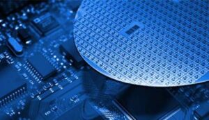
Advanced packaging is becoming increasingly important in semiconductor manufacturing as it allows for more compact, efficient, and powerful chips. As traditional transistor scaling becomes ever more challenging, advanced packaging has emerged as a critical area of innovation. Advanced packaging techniques, such as 3D integration, allow multiple chips to be stacked and interconnected, enhancing performance and reducing latency. As chip architectures continue to evolve, advanced packaging is key to overcoming the limitations of traditional scaling methods, such as lithography.

Chiplet integration on a wafer enabled by collective die-to-wafer hybrid bonding (Source: EV Group (EVG))
One of the most significant advances in packaging is 3D packaging, where multiple chips are stacked on top of each other and interconnected vertically. This approach reduces the physical footprint of devices while increasing performance by shortening the distance between components. In addition, 3D stacking allows for heterogeneous integration, where chips with different functionalities (e.g., processors, memory, sensors) can be combined in a single package.
Rather than designing a single monolithic chip, chiplets are small, modular pieces that can be combined to create a custom chip. This approach offers flexibility, allowing companies to mix and match different types of chips based on specific requirements. Chiplets are particularly beneficial for scaling production and improving yields by enabling smaller, more manageable chip designs. The development of standardized interfaces for chiplets is fostering a more collaborative ecosystem among manufacturers.
Currently, advanced packaging technologies are used across a variety of industries that require high-performance, efficient, and compact solutions. Consumer electronics, such as smartphones, tablets and wearables, benefit from advanced packaging, which enables smaller, more powerful devices with extended battery life. In automotive, with the rise of electric vehicles (EVs) and autonomous driving systems, advanced packaging helps integrate complex electronic systems within the limited space of a vehicle. Healthcare, in particular, medical devices, such as portable diagnostic tools and implants, rely on advanced packaging for miniaturization and enhanced functionality. Aerospace and defense utilize advanced packaging to meet the demands of high-performance computing (HPC) in compact, rugged environments.
The versatility of advanced packaging allows for expansion into emerging markets. Advanced packaging can enable compact, energy-efficient solutions needed for the abundance of Internet of Things (IoT) devices in the IoT sector. 5G infrastructure requires advanced packaging for the development of 5G networks, supporting the integration of more components in a smaller form factor. Quantum computing will rely on advanced packaging to play a crucial role in integrating quantum components with traditional electronics. AI edge devices can benefit from advanced packaging by integrating more processing power in a confined space, enhancing performance and reducing latency.
Advanced packaging technologies are expected to revolutionize the way chips are designed and manufactured. By enabling higher performance and lower power consumption, these techniques will drive the next wave of innovation in the semiconductor industry. In 2025, we can expect to see continued investment in these packaging techniques, which will enable chips to perform better while maintaining or even reducing their physical size. The ability to integrate multiple functionalities into a single package will unlock new possibilities in consumer electronics, automotive, healthcare, and more.
Photonic integrated chips (PICs) and optical interconnects answer the call to enable faster data transfers. As data volumes continue to increase and communication speeds continue to accelerate, the need for faster and more efficient interconnects has never been greater. Traditional electrical interconnects are reaching their limits in terms of bandwidth and power consumption, leading to the rise of PICs and optical interconnects.
PICs use light to transmit and process data instead of electrical signals. By leveraging the speed and bandwidth of light, photonic chips can provide much faster data transfer rates while consuming less power than traditional electrical chips. This makes them ideal for applications that require high-speed processing, such as data centers, AI, and telecommunications.
Optical interconnects are used to link different components of a chip or between chips in a system. These interconnects can handle much larger data transfer rates than electrical interconnects, reducing the need for complex and power-hungry wiring. Optical interconnects also have the potential to reduce latency in communication between different components, enabling faster processing speeds.
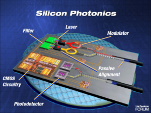
Illustration of silicon photonics device (Source: Photonic Network Communications, Researchgate)
Recent advancements in PICs have focused on improving the efficiency of light sources, such as lasers, and enhancing modulators and detectors integrated on a single chip. Fabrication techniques have also evolved to support these advancements. Innovations in lithography, etching, and deposition processes have enabled the precise creation of intricate optical structures, enhancing the performance and scalability of PICs.
PICs are transforming multiple industries by offering solutions for high-speed data transfer and low-latency communication. PICs are revolutionizing data centers by enabling faster, more energy-efficient interconnections between servers. This capability supports the growing data demands of cloud computing and big data analytics. The telecommunications sector benefits from PICs in fiber optic networks where they provide higher data transmission rates and increased network reliability, crucial for the rollout of 5G and future communication technologies. In healthcare, PICs are enhancing medical imaging systems and diagnostics. Their high data bandwidth and precision enable better resolution and faster processing in applications like optical coherence tomography (OCT) and photonic biosensors. In defense and aerospace, PICs are employed in advanced communication systems and sensors, offering enhanced performance in rugged environments and reducing the size and weight of equipment.
The versatility of PICs paves the way for their expansion into emerging markets, offering new applications and opportunities. For autonomous vehicles, PICs can be integrated into LiDAR systems, which are essential for object detection and navigation, providing superior resolution and faster data processing. In AI systems, PICs can significantly accelerate data transmission within high-performance computing clusters, enhancing machine learning model training and inference capabilities. Consumer electronics benefit as PICs have great potential for augmented reality (AR) and virtual reality (VR) devices, where high-speed, low-latency optical connections can improve user experiences by enabling higher resolution and more responsive interactions. PICs will aid quantum computing particularly in developing quantum communication networks and interfacing qubits with classical control systems.
The integration of photonic components into traditional semiconductor processes is expected to drive significant advancements in the industry. By enabling faster data transmission and lower power consumption, PICs will support the development of next-generation data-intensive applications. This trend will likely lead to new partnerships between semiconductor and telecommunications companies, spurring innovation and competition.
Artificial intelligence is one of the most transformative technologies of the 21st century, and its impact on the semiconductor industry is nothing short of profound. As AI workloads become more complex, there is a growing need for processors that are specifically designed to handle the unique requirements of AI algorithms. AI-specific processors are optimized to accelerate tasks such as machine learning, neural networks, and natural language processing, enabling faster and more efficient AI computation.
Graphics processing units (GPUs) have long been used for AI and machine learning tasks due to their parallel processing capabilities. In 2025, GPUs will continue to evolve to support more advanced AI workloads, with higher processing power, greater memory bandwidth, and specialized AI cores for faster neural network training and inference.
Tensor Processing Units (TPUs) are custom-designed processors developed by Google specifically for machine learning applications. These processors are optimized for tensor computations, which are central to many AI algorithms. TPUs offer significant speed and efficiency advantages over traditional CPUs and GPUs in AI tasks and will continue to see widespread adoption in AI-driven applications.
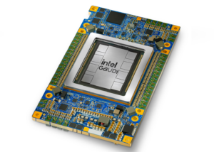
Intel Gaudi 3 AI accelerator chip (Source: CDO Trends)
AI accelerators are chips designed to handle specific AI tasks more efficiently. These accelerators can be used in a variety of applications, from edge devices (such as smartphones and IoT devices) to large-scale data centers. As soon as this year, AI accelerators will become more powerful and ubiquitous, enabling AI processing in real-time for a wide range of use cases.
AI-specific processors are transforming the semiconductor industry by driving the development of custom chips tailored to the needs of AI workloads. These processors will continue to push the boundaries of performance, enabling faster and more efficient AI models. As AI becomes increasingly integrated into industries such as healthcare, automotive, and finance, the demand for specialized AI processors will continue to grow, creating new opportunities for semiconductor manufacturers.
The surge in demand for AI coupled with HPC, which provides the data processing, is pushing semiconductor companies to innovate in chip design and architecture. Companies like NVIDIA, AMD, and TSMC are at the forefront, developing chips that cater to these high-demand sectors. AI and HPC technologies are already integrated across various industries. AI is revolutionizing healthcare through medical diagnostics, personalized medicine, and drug discovery, while HPC enables complex genomic analysis and simulations. Autonomous vehicles rely heavily on AI for decision-making processes, and HPC is crucial for the development and testing of autonomous systems. The financial services groups are using AI algorithms for fraud detection, risk management, and algorithmic trading, all of which is supported by HPC for real-time data processing. Manufacturing is progressing by using AI-powered predictive maintenance and quality control, which is transforming industrial processes. HPC is used to facilitate large-scale simulations and optimizations in the manufacturing environment. AI enhances customer experience through personalized recommendations and demand forecasting for retailers using this technology.
Where do we go from here? AI and HPC will play a crucial role in managing smart city infrastructure, including traffic management, energy distribution, and public safety. Agriculture and precision farming, powered by AI, will optimize crop yields and resource usage, with HPC supporting large-scale environmental data analysis. AI-driven personalized learning platforms and HPC-enabled virtual labs will transform the educational landscape, making learning more adaptive and accessible. For the entertainment industry, AI is being used in content creation, recommendation systems, and gaming, while HPC supports rendering and simulation processes in visual effects and virtual reality. The growth of AI is expected to significantly impact the semiconductor industry by driving investments in research and development and influencing market dynamics.
The semiconductor industry is undergoing a rapid evolution driven by several key trends, including innovations in advanced packaging techniques, photonic chips and optical interconnects, and AI-specific processors. These advancements are not only reshaping the way chips are designed and manufactured but are also enabling the development of new applications that will transform industries and everyday life.
This year, the semiconductor industry will continue to evolve, driven by the need for faster, more efficient, and more powerful devices. As these emerging technologies mature, they will play a critical role in shaping the future of computing, communications and AI, opening up new possibilities and opportunities for innovation. Semiconductor manufacturers who invest in these trends will be at the forefront of this transformation, leading the way into a new era of technological advancement. I am very much looking forward to all of the new applications we will see this year.
(Source: The Digital Speaker)